- 您现在的位置:买卖IC网 > Sheet目录2011 > MAX5893EGK+D (Maxim Integrated Products)IC DAC 12BIT DUAL 500MSPS 68-QFN
Address 07h
Bit 7
Logic 0 (default) adds the 10 bits offset cur-
rent to OUTIN. A logic 1 adds the 10 bits off-
set current to OUTIP.
Address 08h
Bits 7–0
These 8 bits define the binary number for
fine-gain adjustment of the QDAC full-scale
current (see the
Gain Adjustment section). Bit
7 is the MSB. Default is all zeros.
Address 09h
Bits 3–0
These 4 bits define the binary number for the
coarse-gain adjustment of the QDAC full-
scale current (see the
Gain Adjustment sec-
tion). Bit 3 is the MSB. Default is all ones.
Address 0Ah, Bits 7 to 0; Address 0Bh, Bit 1 and Bit 0
These 10 bits represent a binary number that
defines the magnitude of the offset added to
the QDAC output (see the
Offset Adjustment
section). Default is all zeros.
Address 0Bh
Bit 7
Logic 0 (default) adds the 10 bits offset to
OUTQN. A logic 1 adds the 10 bits offset to
OUTQP.
Offset Adjustment
Offset adjustment is achieved by adding a digital code
to the DAC inputs. The code OFFSET (see equation
below), as stored in the relevant control registers, has a
range from 0 to 1023 and a sign bit. The applied DAC
offset is 4 times the code stored in the register, provid-
ing an offset adjustment range of ±255 LSB codes. The
resolution is 1 LSB.
Gain Trim
Gain trimming is done by varying the full-scale current
according to the following formula:
where IREF is the reference current (see the Internal
Reference section). COARSE is the register content of
registers 05h and 09h for the I- and Q-channel, respec-
tively. FINE is the register content of register 04h and
08h for the I- and Q-channel, respectively. The range of
coarse is from 0 to 11, with 11 being the default. The
range for FINE is from 0 to 255 with 0 being the default.
Given this, the gain can be adjusted in steps of approx-
imately 0.01dB.
Single-Port/Dual-Port Data Input Modes
The MAX5893 is capable of capturing data in single-
port and dual-port modes (selected through bit 6,
address 02h). In single-port mode, the data for both
channels is input through the A port (A11–A0).
The channel for the input data is determined through
the state of the SELIQ/B11 (pin 26) bit. When SELIQ is
set to logic-high, the input data is presented to the
I-channel, when set to logic-low, the input data is
presented to the Q-channel. The unused B-port inputs
(DATACLK/B10, B9–B0) should be grounded when run-
ning in single-port mode.
Dual-port mode, as the name implies, requires that
each channel receives its data from a separate data
bus. SELIQ/B11 and DATACLK/B10 revert to data bit
inputs for the Q-channel in dual-port mode.
The MAX5893 control registers can be programmed to
allow either signed or unsigned binary format (bit 7,
address 02h) data in either single-port or dual-port
mode. Table 3 shows the corresponding DAC output
levels when using signed or unsigned data modes.
Data Synchronization Modes
Data synchronization circuitry is provided to allow oper-
ation with an input data clock. The data clock must be
frequency locked to the DAC clock (fDAC), but can
have arbitrary phase with respect to the DAC clock.
The synchronization circuitry allows for phase jitter on
the input data clock of up to ±1 data clock cycles.
Synchronization is initially established when the reset
pin is asynchronously deasserted and the input data
clock has been running for at least 4 clock cycles.
Subsequently, the MAX5893 monitors the phase rela-
I
COARSE
I
FINE
OUTFS
REF
=
×
+
×
3
4
1
16
3
32
256
1024
24
I
OFFSET
I
OFFSET
OUTFS
=
×
4
2
16
MAX5893
12-Bit, 500Msps Interpolating and Modulating
Dual DAC with CMOS Inputs
______________________________________________________________________________________
17
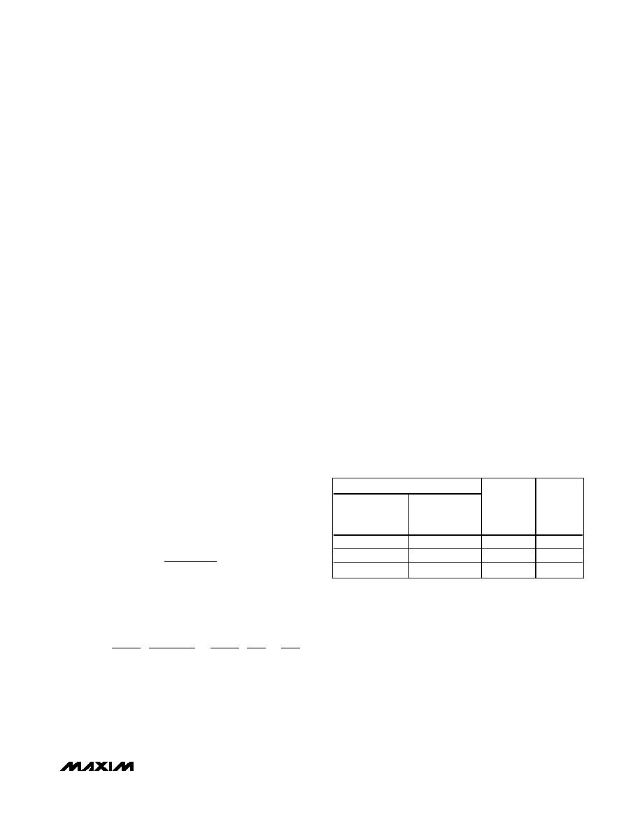
DIGITAL INPUT CODE
OFFSET
BINARY
(UNSIGNED)
TWO'S
COMPLEMENT
(SIGNED)
OUT_P
OUT_N
0000 0000 0000
1000 0000 0000
0
IOUTFS
0111 1111 1111
0000 0000 0000
IOUTFS/2
1111 1111 1111
0111 1111 1111
IOUTFS
0
Table 3. DAC Output Code Table
发布紧急采购,3分钟左右您将得到回复。
相关PDF资料
MAX5894EGK+D
IC DAC 14BIT DUAL 500MSPS 68-QFN
MAX5895EGK+D
IC DAC 16BIT 500MSPS DUAL 68-QFN
MAX5898EGK+D
IC DAC 16BIT DUAL 500MSPS 68-QFN
MAX6900ETT+T
IC RTC I2C COMPAT 6-TDFN
MAX6902ETA+T
IC RTC SPI COMPAT 8-TDFN
MAX7375AXR604+T
IC OSC SILICON SC70-3
MAX7394ATTLY+T
IC OSC SILICON 922KHZ 6-TDFN
MAX7403CSA+
IC FILTER LOWPASS 8-SOIC
相关代理商/技术参数
MAX5893EGK+TD
功能描述:数模转换器- DAC 12-Bit 2Ch 500Msps DAC RoHS:否 制造商:Texas Instruments 转换器数量:1 DAC 输出端数量:1 转换速率:2 MSPs 分辨率:16 bit 接口类型:QSPI, SPI, Serial (3-Wire, Microwire) 稳定时间:1 us 最大工作温度:+ 85 C 安装风格:SMD/SMT 封装 / 箱体:SOIC-14 封装:Tube
MAX5893EGK-D
功能描述:数模转换器- DAC RoHS:否 制造商:Texas Instruments 转换器数量:1 DAC 输出端数量:1 转换速率:2 MSPs 分辨率:16 bit 接口类型:QSPI, SPI, Serial (3-Wire, Microwire) 稳定时间:1 us 最大工作温度:+ 85 C 安装风格:SMD/SMT 封装 / 箱体:SOIC-14 封装:Tube
MAX5893EGK-TD
功能描述:数模转换器- DAC RoHS:否 制造商:Texas Instruments 转换器数量:1 DAC 输出端数量:1 转换速率:2 MSPs 分辨率:16 bit 接口类型:QSPI, SPI, Serial (3-Wire, Microwire) 稳定时间:1 us 最大工作温度:+ 85 C 安装风格:SMD/SMT 封装 / 箱体:SOIC-14 封装:Tube
MAX5893EVCMOD2
功能描述:数模转换器- DAC Evaluation Kit for the MAX5893/MAX5894/MAX5895 RoHS:否 制造商:Texas Instruments 转换器数量:1 DAC 输出端数量:1 转换速率:2 MSPs 分辨率:16 bit 接口类型:QSPI, SPI, Serial (3-Wire, Microwire) 稳定时间:1 us 最大工作温度:+ 85 C 安装风格:SMD/SMT 封装 / 箱体:SOIC-14 封装:Tube
MAX5893EVKIT
功能描述:数模转换器- DAC Evaluation Kit for the MAX5893/MAX5894/MAX5895 RoHS:否 制造商:Texas Instruments 转换器数量:1 DAC 输出端数量:1 转换速率:2 MSPs 分辨率:16 bit 接口类型:QSPI, SPI, Serial (3-Wire, Microwire) 稳定时间:1 us 最大工作温度:+ 85 C 安装风格:SMD/SMT 封装 / 箱体:SOIC-14 封装:Tube
MAX5894EGK+D
功能描述:数模转换器- DAC 14-Bit 2Ch 500Msps DAC RoHS:否 制造商:Texas Instruments 转换器数量:1 DAC 输出端数量:1 转换速率:2 MSPs 分辨率:16 bit 接口类型:QSPI, SPI, Serial (3-Wire, Microwire) 稳定时间:1 us 最大工作温度:+ 85 C 安装风格:SMD/SMT 封装 / 箱体:SOIC-14 封装:Tube
MAX5894EGK+TD
功能描述:数模转换器- DAC 14-Bit 2Ch 500Msps DAC RoHS:否 制造商:Texas Instruments 转换器数量:1 DAC 输出端数量:1 转换速率:2 MSPs 分辨率:16 bit 接口类型:QSPI, SPI, Serial (3-Wire, Microwire) 稳定时间:1 us 最大工作温度:+ 85 C 安装风格:SMD/SMT 封装 / 箱体:SOIC-14 封装:Tube
MAX5894EGK-D
功能描述:数模转换器- DAC RoHS:否 制造商:Texas Instruments 转换器数量:1 DAC 输出端数量:1 转换速率:2 MSPs 分辨率:16 bit 接口类型:QSPI, SPI, Serial (3-Wire, Microwire) 稳定时间:1 us 最大工作温度:+ 85 C 安装风格:SMD/SMT 封装 / 箱体:SOIC-14 封装:Tube